
")
Fast delivery within 72 Hours
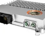
B&R X90CP154.60-00
Rated 5.00 out of 5 based on 1 customer rating
(1 customer review)
X90 mobile controller, ARM Cortex A9-650, 256 MB DDR3 RAM, 32 kB FRAM, 4 GB flash memory, 1 POWERLINK to M12, 1 Ethernet 10/100BASE-T to M12, 3 CAN on CMC header, 1 LIN on CMC header, 1 RS232 on CMC h…
Request for Quote
Shipping & Delivery
-
 Courier delivery
Our courier will deliver to the specified address
5-6 Days
From €20
-
 DHL Courier delivery
DHL courier will deliver to the specified address
2-3 Days
From €40
-
 Warranty 1 year
-
 Free 30-Day returns
Description
X90 mobile controller, ARM Cortex A9-650, 256 MB DDR3 RAM, 32 kB FRAM, 4 GB flash memory, 1 POWERLINK to M12, 1 Ethernet 10/100BASE-T to M12, 3 CAN on CMC header, 1 LIN on CMC header, 1 RS232 on CMC header, 60 multifunction I/O, 1 sensor power supply, die-cast aluminum housing, service access window, LED status indicators
Specification
| Interfaces | 1x Ethernet/POWERLINK (switchable), 1x POWERLINK, 3x CAN bus, 1x LIN bus, 1x RS232, 1x USB |
|---|---|
| System module | Controller |
| Insulation voltage for GND and housing | 500 Veff |
| B&R ID code | 0x29AD |
| Cooling | Fanless |
| Status indicators | Controller function, operating mode, overtemperature, Ethernet, POWERLINK |
| Module run/error | Yes, using LED status indicator, software and diagnostic output |
| CPU function | Yes, using LED status indicator |
| Ethernet | Yes, using LED status indicator |
| Controller redundancy | No |
| Storage health data support | Yes |
| ACOPOS support | Yes |
| ReACTION-capable I/O channels | No |
| Visual Components support | Yes |
| Power consumption | CPU at Ue = 9 / 32 V: 4.8 / 6.0 W |
| CE | Yes |
| UKCA | Yes |
| CRA (Cyber Resilience Act) | In preparation |
| Input voltage | 9 to 32 VDC |
| Nominal voltage 12 V | 9 to 16 VDC |
| Nominal voltage 24 V | 16 to 32 VDC |
| Reset switching threshold | 5.4 V |
| V_CPU | No, required fuse 5 A slow-blow |
| V_I/O | No, required fuse 10 A slow-blow per connection pin |
| Overvoltage | Max. 48 V |
| Overvoltage protection | Load dump pulse A 202 V Ri = 4 Ω |
| Reverse polarity protection | Max. -48 V |
| Real-time clock | Resolution 1 s, retention min. 48 hours, typ. 250 hours at 25°C, precision ±30 ppm over the entire temperature range |
| FPU | Yes |
| Type | CAN bus |
| Clock frequency | 650 MHz |
| Data code | 32 kB |
| Program code | 32 kB |
| L2 cache | 512 kB |
| Integrated I/O processor | Processes I/O data points in the background |
| Option boards | Not available |
| Remanent variables | 32 kB FRAM, retention >10 years |
| Shortest task class cycle time | 400 µs |
| RAM | 256 MB DDR3 SDRAM |
| Data retention | 10 years |
| Guaranteed | 100 TB |
| Results for 5 years | 54.8 GB/day |
| Guaranteed erase/write cycles | 100,000 |
| Error-correcting code (ECC) | Yes |
| Variant | Connection A2 – Source |
| Max. distance | 1000 m |
| Transfer rate | Max. 1 Mbit/s |
| Line length | Max. 100 m between 2 stations (segment length) |
| Physical layer | 100BASE-TX |
| Half-duplex | Yes |
| Full-duplex | No |
| Autonegotiation | Yes |
| Auto-MDI/MDIX | Yes |
| Fieldbus | POWERLINK managing or controlled node |
| Max. output current | 500 mA |
| Connection designation | CAN3 |
| Terminating resistor | External 120 Ω must be provided. |
| Quantity | 1 |
| Function | Digital output 6 A nominal current, push-pull circuit, integrated output protection per channel, configurable overload monitoring per channel, central cutoff via relay,parallel connection, current measurement, error state with configurable error filter. PWM output 6 A nominal current, PWM frequency 15 Hz to 4 kHz, 8 kHz in full-bridge mode, push-pull circuit, integrated output protection per channel, configurable overload monitoring per channel, central cutoff via relay, parallel connection, current measurement, configurable load current distribution of the PWM outputs, dither. Digital input Sink/Source circuit configurable per channel, configurable software input filter |
| Functions | Digital output: 4 A nominal current, source circuit, integrated output protection per channel, configurable overload monitoring per channel, central cutoff via relay, parallel connection, current measurement, error state with configurable error filter. Digital input: Sink/Source circuit configurable per channel, configurable software input filter |
| Nominal voltage | 12 / 24 VDC |
| Input current at 24 VDC | MF-DI (CI + std): Typ. 1.1 / 2.5 mA, configurable MF-AI (AT + PVG): Typ. 1.1 / 5.3 mA, configurable MF-AI (std): Typ. 1.1 mA MF-DO (std): Typ. 2.5 mA MF-PWM (all): Typ. 2.5 mA |
| Input circuit | Sink/Source, configurable |
| Hardware | MF-DI: 3 µs MF-AI (all): 300 µs MF-DO: 150 µs MF-PWM (bridge): 200 µs MF-PWM (std): 150 µs |
| Software | Default 1 ms, configurable between 0 and 25 ms in 0.1 ms increments |
| Input resistance | MF-DI (CI + std): Typ. 9.15 / 20.2 kΩ, configurable MF-AI (AT + PVG): Typ. 4.42 / 22.1 kΩ, configurable MF-AI (std): Typ. 22 kΩ MF-DO (std): Typ. 9.15 kΩ MF-PWM (all): Typ. 9.15 kΩ |
| Input frequency | MF-DI: Max. 50 kHz |
| Switching threshold | MF-DI: 50% of supply voltage MF-AI (all): Switching threshold and hysteresis configurable with software MF-DO: 40% supply voltage MF-PWM (all): 40% supply voltage |
| Input | 0 to 10 V / 0 to 32 V / 0/4 to 20 mA / 0 to 4000 Ω / Temperature inputs (Pt1000 characteristic curve) |
| Digital converter resolution | 12-bit |
| Conversion time | MF-PWM (bridge): 40 μs MF-PWM (std): 80 µs |
| Data type | INT |
| Voltage | 5/10 V |
| Current | Max. 400 mA ±3% |
| Resistance | <0.018%/°C |
| Temperature input | <0.027%/°C |
| Measuring current resistance / Temperature input | <2.2 mA |
| Open-circuit detection | From the application |
| Conversion procedure | SAR |
| Input filter | First-order low-pass filter / cutoff frequency of voltage input 350 Hz, current input 200 Hz |
| Gain | MF-PWM (bridge): <0.5% MF-PWM (std): <3% |
| Offset | MF-PWM (bridge): <0.25% MF-PWM (std): <1.5% |
| Nonlinearity | <0.05% (resistance) <0.2% (temperature inputs) |
| Switching voltage | MF-DO, MF-PWM: V_IO -15% MF-PVG, MF-AI (ratiometric output) : V_CPU – 15% |
| Nominal output current | MF-DO: 4 A MF-PWM (bridge): 6 A MF-PWM (std): 4 A |
| Output protection | Thermal shutdown in the event of overcurrent or short circuit, integrated protection for switching inductive loads |
| Diagnostic status | Overload |
| Leakage current when the output is switched off | MF-DO: Typ. 10 μA, max. 4.1 mA MF-PWM (bridge): Typ. 20 μA, max. 4.1 mA MF-PWM (std): Typ. 10 μA, max. 4.1 mA |
| RDS(on) | 1.4 Ω |
| Residual voltage | <1 V at 4 A nominal current |
| Peak short-circuit current | 50 A (max. 0.2 ms) |
| Resistive load | MF-DO: Max. 250 Hz |
| Inductive load | MF-DO: Load current 4 A: Max. 4 mH (see section “Switching inductive loads”) |
| Braking voltage when switching off inductive loads | MF-DO: Typ. 64 VDC MF-PWM (std): Typ. 64 VDC |
| Switching delay | MF-DO: Max. 150 μs MF-PWM (all): Max. 150 μs |
| Nominal | 9 to 32 VDC |
| Sampling time | MF-DO: 160 μs MF-PWM (bridge): 40 µs MF-PWM (std): 80 μs |
| Current measurement range | MF-PWM (bridge): ±10 A MF-PWM (std): 10 A |
| Resolution | INT MF-PWM (bridge): INT 0x8001 to 0x7FFF / 1 LSB = 305 μA MF-PWM (std): INT 0x0000 to 0x7FFF / 1 LSB = 305 μA |
| Max. gain drift | MF-PWM (bridge): <0.04%/°C MF-PWM (std): <0.2%/°C |
| Max. offset drift | MF-PWM (all): <0.005%/°C |
| Supply voltage (permissible range) | 9 to 32 VDC |
| PWM frequency | MF-PWM (bridge): 15 Hz to 4 kHz MF-PWM (std): 15 Hz to 1 kHz |
| Duty cycle | PWM (bridge): 0 to 32767 or -32767, min. resolution 160 ns depending on PWM frequency PWM (std): 0 to 32767, min. resolution 160 ns depending on PWM frequency |
| Common mode error | MF-PWM (all): 0.01%/V |
| Max. continuous current | 20 mA |
| Complete system | Max. 30 A |
| Inrush current | Typ. 500 A for <300 µs |
| Electrical isolation | Ethernet (IF2) and POWERLINK (IF3) isolated from each other and from other interfaces |
| Any | Yes |
| Installation elevation above sea level | Max. 4000 m |
| Degree of protection per EN 60529 | IP69K |
| Horizontal mounting orientation | -40 to 85°C housing surface |
| Vertical mounting orientation | -40 to 85°C housing surface |
| Derating | See section “Derating”. |
| Storage | 5 to 95%, non-condensing |
| Transport | 5 to 95%, non-condensing |
| Operation | 5 to 100%, condensing |
| Width | 225 mm |
| Length | 219.5 mm |
| Height | 43.5 mm |
| Weight | Max. 1740 g |
| Content of delivery | 2x protective covers for unused female M12 connectors |
Customer Reviews
5
Rated 5 out of 5
1 review
Rated 5 out of 5
1
Rated 4 out of 5
0
Rated 3 out of 5
0
Rated 2 out of 5
0
Rated 1 out of 5
0
1 review for B&R X90CP154.60-00
Clear filters
Add a review Cancel reply
[email protected] –
Awesome